InsightEdge Semiconductors

Deploy enterprise-grade AI directly on your network — AI that never leaves the fab. Build custom models, maintain complete data privacy, and scale without limits, all within your existing infrastructure. Now, accelerate semiconductor innovation with built-in intelligence.

On-Premise Power

100%
Data Control

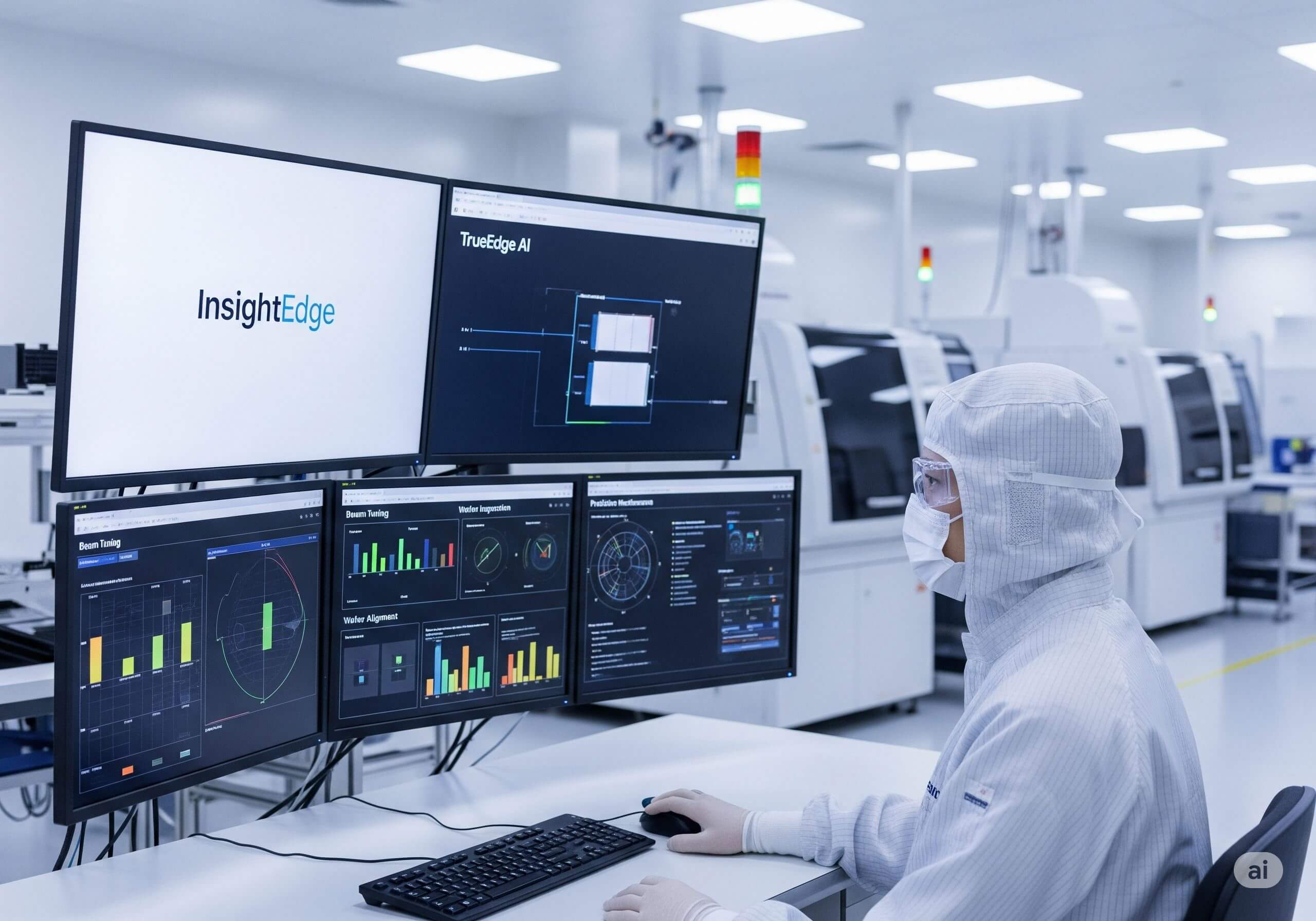
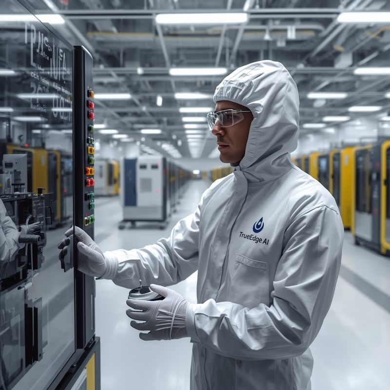
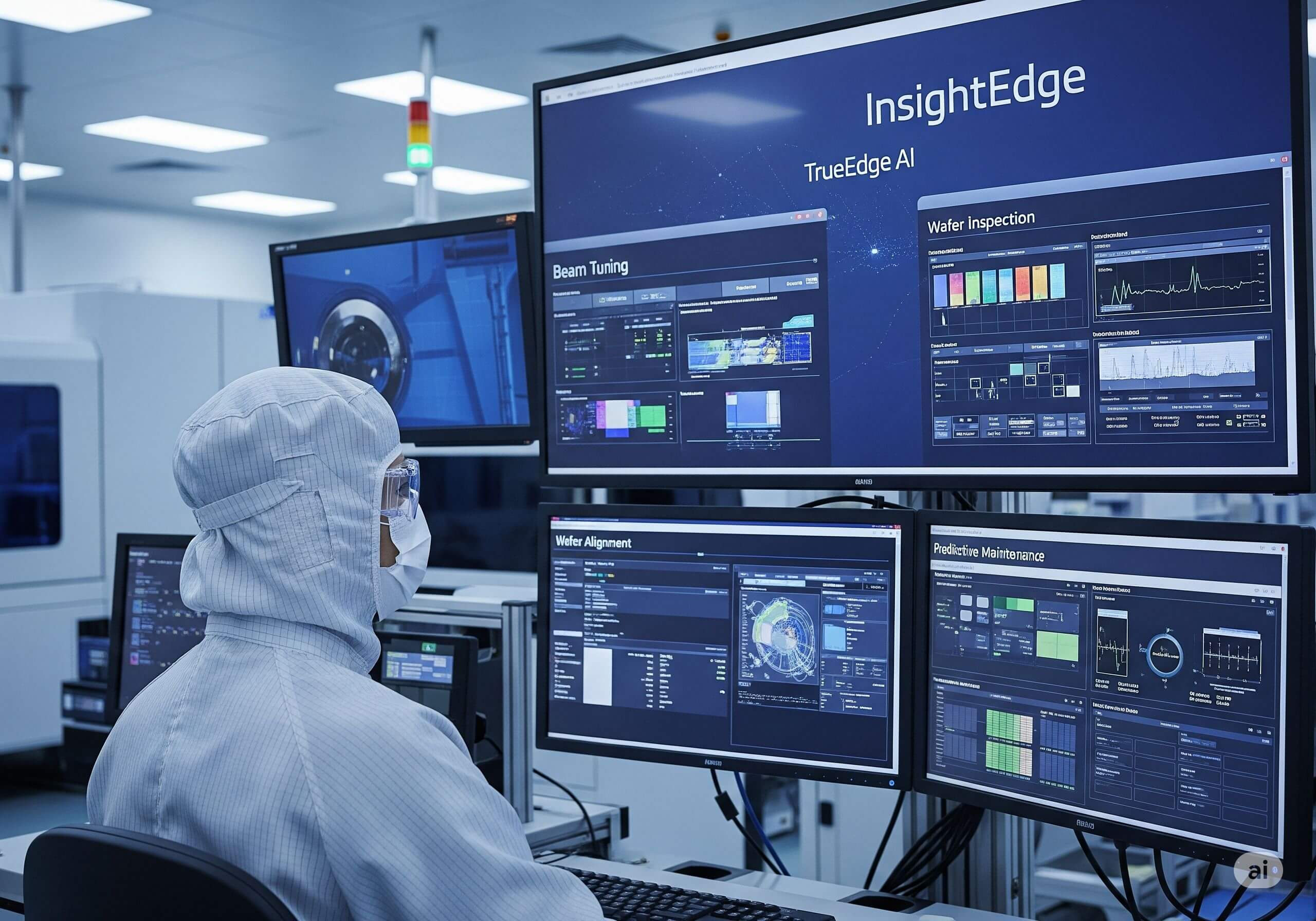
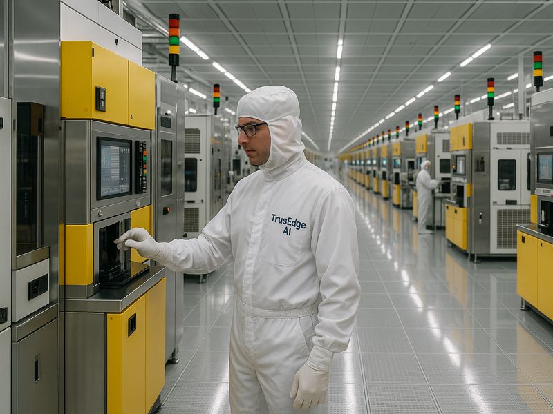
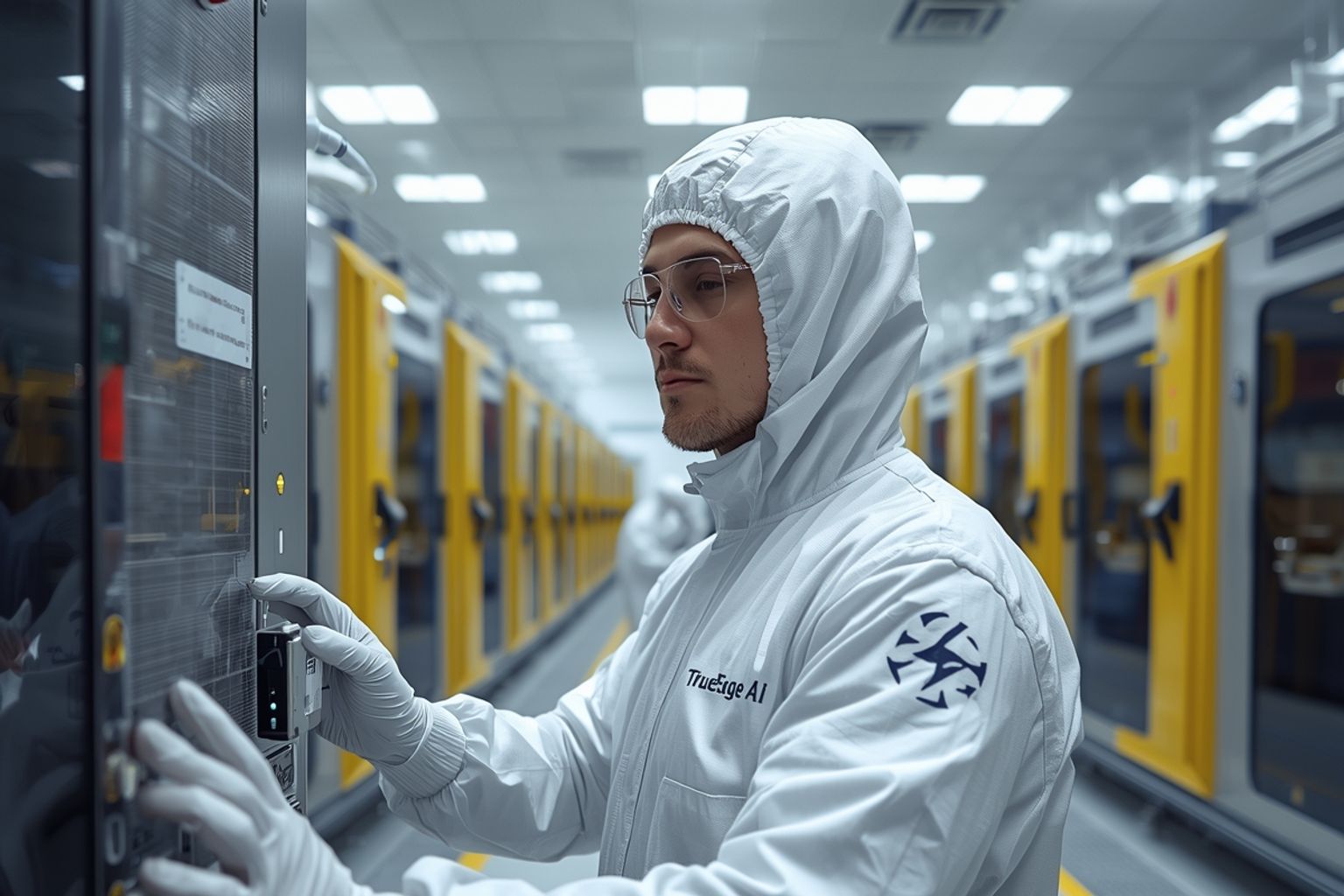
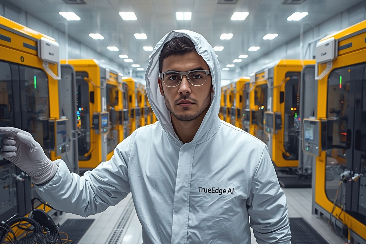
Semiconductor Manufacturing with InsightEdge

With InsightEdge, semiconductor companies can stay ahead of rapidly evolving technology demands accelerating production, ensuring higher yields, and unlocking new possibilities in chip design and manufacturing.

InsightEdge Technology

Advanced Manufacturing

AI-powered semiconductor fabrication

Intelligence Across Every Critical Tool

Ion Implanters

Ion implantation is one of the most critical and most sensitive steps in semiconductor fabrication. Precision in beam energy, angular distribution, and dose control directly impacts device performance and yield.

  • Angular Energy Filtering:
    The Angular Energy Filter (AEF) selectively transmits ions of the correct energy and incident angle while suppressing contaminants and unwanted trajectories.
  • Beam Uniformity Optimization: AI models continuously monitor beam optics (energy spread, divergence, and angle of incidence) to ensure uniform dopant distribution across wafers.
  • RealTime Beam Tuning: Machine learning, deep learning, transformer models, agentic AI, generative AI, and reinforcement learning algorithms adaptively tune beam parameters during high-dose implants, ensuring stable current, precise dose control, and continuous optimization of implantation conditions.
  • Contaminant Suppression:The AEF mitigates the risk of low-energy tails and angular straggle, reducing junction leakage and device variability.
  • Predictive Maintenance for Beamlines: AI models track wear and performance degradation across beamlines, ion sources, angular energy filters (AEF), SCARA robotic arms, electrostatic wafer chucks (ESC), and endpoint detection systems predicting when replacements or calibrations are required to avoid unplanned downtime.
Ion Implantation Process

Precision Control

AI-optimized beam parameters

Semiconductor Manufacturing

EUV Lithography Systems

Critical for advanced nodes where nanometer-level precision is essential.

  • AI-Guided Exposure Control
  • Contamination & Optics Monitoring
  • Stability Monitoring

Etch & Deposition Tools

Core to material patterning and growth processes.

  • Plasma Optimization
  • Drift & Instability Detection
  • Predictive Maintenance
Manufacturing Process

Process Optimization

Real-time monitoring and control

CMP & Wafer Handling

Ensures surface integrity and wafer transport reliability.

  • Pad & Slurry Monitoring
  • Robotic Arm Alignment
  • Planarization Control

Inspection & Metrology Systems

Provides advanced defect detection and classification.

  • Deep Learning Defect Classification
  • Pattern Variation Detection
  • Critical Defect Prioritization
Inspection Systems

Quality Assurance

AI-powered defect detection

Key Features

Key Features

Core Capabilities

Comprehensive AI solutions

  • Smart Fabrication: Optimize process parameters in real time across ion implantation, EUV, etch, and CMP.
  • Beam & Process Optimization: Maximize uniformity and throughput while reducing variability.
  • Predictive Maintenance: Anticipate failures in high-value tools before they occur, minimizing downtime.
  • AI-Powered Inspection: Classify and prioritize defects with higher accuracy for faster yield learning.
  • On-Premise Security: AI models run fully within fab infrastructure for total compliance and IP protection.

Business Impact & Use Cases

  • Yield Improvement: Detect and fix micro-defects before they propagate through wafers.
  • Reduced Downtime: Predict failures in implanters, EUV, and CMP before they happen.
  • Cost Savings: Extend equipment lifetime and minimize consumable waste.
  • Time-to-Market Advantage: Accelerate ramp of new technology nodes with adaptive AI models.
  • Scalability: Expand AI across multiple fabs without redesigning infrastructure.
Business Impact

Business Value

Measurable improvements

Why InsightEdge

Our Advantage

Industry-leading technology

Why InsightEdge?

  • Fab-First Architecture: Designed specifically for semiconductor equipment integration.
  • Customizable AI Models: Built to match your fab's unique process flows.
  • Zero Data Leakage: All models run on premise; your process data never leaves the fab.
  • Proven in High-Volume Manufacturing: Deployed across critical fab tools worldwide.
  • Scales Across the Fab: From implanters to CMP, inspection to lithography, one platform covers it all.

Download our white paper to learn how InsightEdge can optimize your fabrication process and boost yields.